 |
 |
 |
 |
 |
 |
|
The non-linear mathematical operators - Multiply and Divide
Previously we looked at what I called the linear maths operators (Add and Subtract). They were Linear, because if you tied the various inputs together and varied them as a single input, the output would still demonstrate a linear relationship to the input. In fairness, we also previously saw the comparator, and the Schmitt trigger. These functions were non-linear like those we are about to see. In that particular case, the outputs were mathematically discontinuous. With abrupt turning points it would not have been possible to describe the output as a continuous function. To do so, we would have had to use some sort of limits and describe the various different linear behaviours discretely.
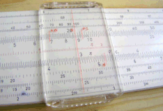
Before the pocket calculator was possible, the slide rule was commonplace. The vernier scale was simply a reflection of log tables, known since at least 1540. With simple addition, and a slide rule, multiplication is possible. This is the approach we'll take here, when multiplying numbers with Op-Amps. First we'll find the log of the input signal, we'll operate on it using the linear operators we've already seen, and then we'll raise the answer to the base of the original logarithm. If we use the summing amplifier, we'll have multiplied overall, and if we use the differential amplifier, then we'll have divided overall. This is shown below. 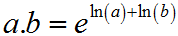 There are other ways to achieve analogue multiplication. Probably the most realistic solution to the multiplication problem, is the four quadrant multiplier. In general terms it's a better solution than the log law scheme that I'll describe here. Unfortunately the four quadrant multiplier doesn't explicitly use Op-Amps, and this is part of a series about Op-Amps. As the article develops, hopefully it'll become clearer when and why one might use an Op-Amp solution for non linear operations, and the disadvantages of so doing. The world of the BJT (Ordinary Transistor)Clearly our first problem is to figure out a way of generating this logarithmic behaviour, so we can exploit the logarithmic identities. In practice, we're going to use the forward biased base/emitter junction of a standard transistor to generate a logarithmic function. As we'll see the logarithmic behaviour comes from the exponential relationship between voltage and current in that PN junction. I've not explained the transistor on this website. The actual operation of the transistor requires a fairly complex dialogue on the atomic structure of matter. Not only is it difficult to describe, it's difficult to understand. Here I describe a simplified model of an NPN transistor which depends on an analogy between fluid, and electron flow. The model works well to a point. I also write here about when and how it fails. The first stage in developing an understanding of the transistor, is to understand the main diode of the transistor. This is the base emitter junction which controls operation . Using the fluid flow analogy this is no different, so we start with the non-return valve.
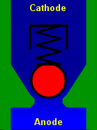
Inside the non return valve, is a valve seat, a valve and a spring. The valve is a small lump of material that sits inside the pipe and can rest against the seat. If water pressure acts in a direction that pushes the valve against the seat, then the valve is forced closed. The harder the water pushes, the more tightly the valve is closed. If water were to push in the other direction then it would lift the valve off its seat, and water would flow. Obviously a problem would be that the valve would disappear off down the pipe with the water, perhaps never to be seen again! A spring is used behind the valve, and that rests against another surface which allows water to pass feely, but prevents the spring and the valve escaping down the pipe. The valve does not need to have a spring, but most do because it helps the operation of the valve. To us, the spring has important mathematical consequences. As the water pressure rises the valve opens more, and more water flows. Unless the force of the water has the capacity to overwhelm the valve, some kind of equilibrium between the water pressure and the spring force will be reached. The harder the water pushes, the more the valve opens. The greater opening increases the flow rate. If there is only a limited ability to supply water, then the water pressure will begin to reduce again. The valve will close slightly. Oscillation in certain circumstances is possible, but equilibrium is just as likely. Overall there will be a balance between the pressure and the flow rate of the water. Unless overwhelmed, the valve will be partly open. The preceding paragraph, describes a diode, as well as a non-return valve, and that is all we need here. In detail it is slightly more complex, but not hugely so. A property of a manufactured semiconductor diode is the "depletion layer" and it is is broadly equivalent to the spring force of the valve on the seat when there is no flow. If we look at the relationship between a diode and the base emitter junction of a transistor there is absolutely no difference as long as the collector of the transistor remains unconnected.
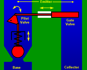
Returning to the valve analogy, we can visualise the same non-return valve and contrast it with a pilot valve. Less people will be familiar with the idea of a pilot valve because it is much less often used. Irrespective, it's the same basic idea as a non return valve. In the pilot valve there would normally be some connections that you don't see in a transistor. We'll ignore those. In our pilot valve, the blob of material that is the pilot valve still has a spring behind it. The movement of the valve is measured by a lever which magnifies the movement of the valve. That magnified movement from the lever actuates the sliding gate of a much bigger valve. The water input port to the pilot valve (base), is small, the input port to the main gate valve (collector) is big. The output of each feeds a single large output port (emitter). This is a pretty good analogy for the basic transistor. The transistor is actually two diodes back to back, and it will behave as such if you test one. Unfortunately if it's connected the wrong way around (swap emitter collector), the gain won't actually be very good because of the internal function and sizing of the transistor regions. That's but a detail. In our pilot valve analogy, the diagram does not show the outputs of the two valves coming together in the emitter port. Actually it's probably just as well. One might be tempted to assume that the restriction that would come about if the two pipes are joined, would allow a large collector flow to alter the pressure balance in the pilot valve. In the mechanical/liquid valve this would happen. In the transistor this effect can only occur if the emitter immediately feeds into a resistor. Such a resistor would provide a feedback mechanism where variations in the collector current could alter the base emitter voltage. Obviously this mechanism can certainly lead to instability in practical transistor circuits. As you can see from the diagram, the flow into the collector port never passes near, let alone through, the base. In a transistor the flow of electrons actually passes through the base region of the device. That too is critical to the operation of the transistor, but it's not shown on the valve analogy diagram. For the time being it's not important. The analogy broadly represents an NPN transistor. The function below describes the basic relationship inside the transistor. hFE (hybrid forward emitter), is the current gain of the device, also known as β. It describes the ratio between the current flow into the base and the collector. In our liquid valve hFE describes the result of measuring the relationship between the pilot valve aperture size and its spring strength, relative to the size and movement of the gate valve in the collector. If you're wondering why β, it's because α is the ratio of the collector and emitter currents. This latter ratio, is just slightly less than 1, but clearly α and β are different ways of expressing the same quantity. 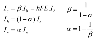 At this point one might reasonably ask where the logarithmic relationship that we need has gone. It's still there, it's just that the expression above only considers flow. As stated, the parameter hFE (β) describes the magnification effect of the pilot, lever and gate on the flow in the collector port. When we set the input to the pilot in terms of a flow rate, it directly relates to some proportional movement of the pilot valve. If we specify the pressure, on the pilot (base), we see a corresponding exponential relationship of flow in the emitter. If we need a logarithmic relationship, then we can control flow into the base and observe a logarithmic relationship to base emitter potential.
Feel free to start thinking of valves as glowy vacuum things again now! At this stage, we can no longer carry the analogy with a mechanical fluid valve. The graph on the right shows the full relationship between the two critical transistor voltages and the collector current, which is the controlled parameter. If you don't use Internet Explorer, you'll actually be able to interact with the graph and spin it around to get a better view from different angles. Normally you would see this as a 2D graph on transistor datasheets for obvious reasons, but it would normally have a few plots on the same chart. These would represent the variable relationship between Vce (Voltage collector-emitter) and Ic (collector current) with at various specific Vbe (Voltage base-emitter) settings. You can see in the 3D plot two different curves, at right angles. They combine to make the surface. When we saw the transistor as a mechanical valve, we looked at one of these relationships, specifically Vbe ~ Ie the pilot valve or diode. This represents the exponential relationship on the 3D graph (obviously multiplied by α). I briefly described how this exponential relationship could be used to develop a logarithmic one by swapping the dependent and independent variables, voltage and current. The logarithmic behaviour shown on the 3D graph is a completely independent relationship. In the mechanical valve, there was a large controlled gate in the collector port. In a general sense the wider this gate, the greater that flow could expected to be. In the real world, liquid flow would be applied and it would have a given pressure. If the valve were to close slightly, then the pressure difference either side of the valve would rise, and the flow rate would fall. If the flow rate were to rise alone then so too would the pressure difference. The problem here is that the relationships are all linear, like resistors. Actually the behaviour of the collector in a real transistor is logarithmic, as can be seen in the 3D graph. As the voltage between the collector and emitter rises, the current does not always follow linearly. The mechanical valve model does not demonstrate this behaviour.
We could modify the mechanical model to exhibit this 'kind of' behaviour but it would always be unrealistic. The non return valve and the pilot of the pilot valve, is a good model for a diode or a base emitter junction. By contrast, it is difficult to develop such a model for the collector behaviour, because of the way that the transistor works. Actually the nearest thing is a device called an injector, which relies on fluid dynamic energy levels, very similar to the bandgap model of the transistor. The injector is a three terminal device like the transistor, but it has an overflow. It won't work in reverse, but it would spill liquid and steam through the overflow. The best way to think about the relationship between Vce and Ic is that the base 'programming' current develops hFE 'chances' for current to flow from the collector to the emitter. If there is little potential pushing electrons to exploit those chances, then no current will flow. Almost as soon as there is any potential (or voltage) on the collector terminal then a considerable current can flow. hFE then, governs the current that flows in the collector when there is sufficient potential for a current to flow. This broadly is the flat part of the graph. It would be untrue to say that Vce does not influence Ic, but its effect is designed to be minimal. Broadly, the larger that the average value Vce is, the smaller the effect of a given ΔVce will be on Ic. It is very common for a transistor to be controlled by voltage, rather than by a current. If there is a useful voltage on the collector, when one linearly increases the voltage on the base, one will see an exponential rise in the collector current which is approximately hFE times the base current. The exponential increase of flow that occurs in the otherwise logarithmic collector comes about because of the exponential rise of current in the base, due to the linear increase in base voltage. Obviously the exponential relationship of voltage and current in the base emitter junction is very important. We already know that this relationship is the same as that of the forward biased diode, and that it is reasonably well described by a mechanical non-return valve. Let's look at the function that describes that relationship. 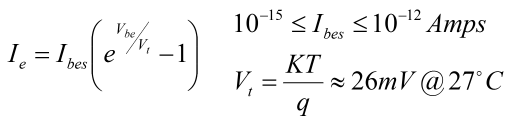 The equation above is the original Shockley diode equation. It attempts to describe the practical forward biased diode. There are some problems, but broadly it works. Vbe is the voltage on the diode, or the base~emitter junction of the transistor. Vt is the thermal voltage. That is derived from a combination of physical properties including the Boltzmann constant and the charge on an electron. Ibes is a value which is represents the reverse saturation current of the specific base emitter junction. If Vt is a real quantity, then Ibes is less so. The trouble here is that the fundamental principles of operation in a semiconductor are so delicate. Small changes in temperature or doping of the semiconductor make huge differences to the behaviour of the semiconductor. The equation can be used to calculate Ibes, but it cannot be expected that Ibes will be appropriate for any other transistor, or even if the temperature of a measured transistor changes. Particularly, it is important to notice that the equation is arranged such that the -1 term makes almost no difference. For the purposes of a practical approximation, it can be ignored. Now there is an understanding about what the transistor is doing, it is easily possible to develop an Op-Amp circuit that exploits transistor behaviour to implement logarithmic operators. The Log amplifierThe circuit below, describes the logarithmic amplifier. From what we saw about the standard inverting amplifier previously, and the transistor above, it's fairly straightforward to describe what is happening. The scheme, as with most op-amp circuits, depends on the virtual ground developed at the inverting input of the amplifier. The amplifier attempts to control the voltage on the inverting input to be the same as that on the non-inverting input.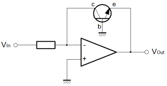 If a voltage is applied at the Vin terminal, then a current will flow in R1 to the virtual ground at the amplifier inverting input. The amplifier inputs are high impedance, so the current that flows in R1 must flow through the collector of T1. The only thing that the amplifier can do, is to generate a voltage drop from the base to the emitter of the transistor. A small current flows from ground down to the amplifier output, due to the Vbe drop. Another current hFE times bigger than this Ib current begins to flow in the collector. The voltage on the amplifier output continues to fall until the collector current is the same as that in R1, so that the virtual ground is maintained. The current through the collector rises more quickly as the base voltage grows linearly. As the collector current rises, the Vbe voltage drop needs to grow less and less to maintain the virtual ground. Consequently, the output voltage from the amplifier has a logarithmic relationship with the input. 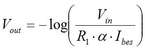 Obviously there is a bit of a proviso here. Strictly there is no logarithm for an input value less than or equal to zero. If a negative input voltage is used then the output of the amplifier will swing to the positive rail and saturate. Should that happen, it is possible that the transistor could become damaged, depending on its type. Practical circuits should provide protection against this eventuality. More important still, the basic design of the circuit is inverting. Although logarithmic the output has the wrong sign for strict correctness. The circuit below is the antilog circuit, and it too is inverting so log and antilog can be cascaded directly. Nevertheless, it is quite important not to forget the sign of the signal. The Antilog amplifierFinally, it's the antilog, or exponential amplifier. The deal here is pretty straightforward. Using the same concept as before but in reverse, the transistor is used to develop an exponential current from a linear voltage input. The exponential current into the virtual ground is balanced by a feedback current in R1. As usual, that keeps the virtual ground at the potential specified by the non-inverting input. 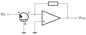 As previously stated, the input to this amplifier is compatible with the output from the logging amplifier. Clearly, the input increases in a negative direction. Like the logging amplifier, it is quite possible to cause a problem with an out of range input. Although the circuit will not convert a positive input voltage, unacceptable bias on the base emitter junction of T1 (forward or reverse) can cause a problem. 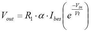 So that's it. I'm sorry this page was a while in arriving. I hope it's worth it! Logging amplifiers can be effectively used to implement analogue multipliers. In this case it might be a good way to implement a squaring circuit, for example. I may take the time to write a page on such a circuit for a practical demonstration. In principle it's straightforward. All you need to do is use the two circuits above, and sandwich a gain of two circuit. Take logs; gain of two, non-inverting amplifier; antilog. This is a circuit from standard blocks that implements an analogue squaring function. Using a summing amplifier the same way, a binary multiplication operator is quite realistic. The only detail, is to carefully scale the sum to the dynamic range available from the chosen transistor. Typically this is four of five decades. The circuit is less suited to a multiplier for, say, a mixer. The Gilbert cell is simpler and more effective for that purpose. In particular, the log law approach to multiplication needs careful scaling. Temperature variations can significantly affect the performance particularly accuracy. From a production perspective it is quite difficult to develop a circuit with consistent behaviour in a batch of boards. This means more calibration effort than is usually desirable. If you want low frequency, wide dynamic range, low volume (manufacture) analogue multiplication, this isn't a bad way to go. |


Copyright © Solid Fluid 2007-2025 |
Last modified: SolFlu Mon, 08 Apr 2013 22:09:35 GMT |