 |
 |
 |
 |
 |
 |
|
Discontinuous operators - Absolute Value
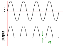
On this page, I'm going to cover the first of the discontinuous mathematical operators. This will conclude in the absolute value circuit but it passes through another related function peculiar to electronics, the precision rectifier. In the most basic sense, the half wave rectifier is simply a diode. An Op-Amp adds the "precision". A simple rectifier diode will usually be arranged with a network of other components. In its simplest form a low voltage non-precision rectifier can be formed using a single diode in a clamp or shunt configuration. It's not usually ideal to short a signal directly to ground through a diode, but it can work. If the diode is strong enough it will have the effect of constraining AC from a push-pull output like an Op-Amp to a positive or negative only signal, depending on the polarity of the diode. Alternatively, in a simple power supply circuit, a single series diode in a step down transformer secondary circuit could feed a smoothing capacitor. This type of circuit will yield a DC supply from AC mains.
In both of these cases, the limitation is that the diode has a forward voltage drop. On the coming page about non-linear operators, we'll see why this drop exists, but for now you might just have to accept that it does. What this means is that the diode is actually a little like a resistor when forward biased with small signals. Obviously when the diode is reverse biased, very little current at all flows. At very low forward voltages not much current flows, until the diode forward voltage is reached, and then suddenly the diode conducts a large current as if it were a simple piece of wire. Another way to look at this is from the perspective of controlled forward current. If the forward current is gradually raised from zero, the voltage across the diode rises in (something like) proportion until the the voltage reaches the diode forward voltage. After that the current can rise a lot and the voltage across the diode changes little. Between zero and the diode forward voltage, the diode behaves something like a resistor in that the current and voltage are related to one another (although the relationship is not linear as it would be with a resistor). The upshot of this non-linear "resistor-esque behaviour" is that a circuit using a diode for rectification will have to accept that the diode forward voltage creeps into the sums. Usually this is highly unwanted. The diode does the broad part of the rectification, but not quite all. Unless one can arrange special power supplies that allow for the forward voltage, clamps never clamp with the desired precision. Precision half wave rectifierThis is where the humble Op-Amp enters from stage left. We've already seen in this series how Op-Amps have a very large gain. Typically this large gain is used in a feedback loop and the programming resistors set the implemented gain. It's a fairly small step to see that if a constant voltage source, say a battery, is added in series with the feedback loop, the massive gain of the amplifier will overcome this newly introduced offset. If the battery is a 1 volt battery then the enormous gain of the amplifier will simply slew an extra volt to ensure that the inverting and non-inverting inputs take on the same potential (within the input offsets). This property is extremely useful to us in respect of the precision rectifier. If we somehow place the diode in an Op-Amp feedback loop, perhaps we can use its capacity to overcome the diode forward voltage and make the performance of the rectifier much closer to perfection. This is demonstrated in the precision half wave rectifier shown below. In this first circuit, we're simply aiming to cut out the positive going haf cycles of a sinewave applied to the input. 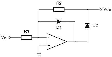 This circuit takes advantage of the slewing property just described. Firstly, let's consider the case where the input voltage trends negative. By inspection we can see that a negative input will tend to force the output of the Op-Amp positive. The forward voltage developed across D2 will cause a current to flow in R2. From there on, it's just the same as we described for the inverting amplifier configuration. The amplifier acts to supply current through R2 which will replace that taken away through R1 to the input. If R1 and R2 are the same value, then the currents through them will be the same, and the overall gain will be unity. The important thing to notice is that the voltage drop across the diode D2 has been automatically compensated because of the large gain in the Op-Amp. The feedback loop acts to balance the current in R1 and R2 so the amplifier automatically develops extra potential at the output to overcome the forward diode drop in D2. Since the output is connected to the loop after D2, the output never sees the diode forward voltage. Finally, the negative input voltage causes the output to rise, so D1 must be reverse biased and can't conduct or affect the output. The other case is where the input voltage rises above zero. Again the amplifier inverts so this time the output of the Op-Amp falls. This time D1 is forward biased. The path through D1 is almost a short. Once the forward voltage of D1 is overcome, the Op-Amp can sink almost any current introduced to the circuit through D1 at this output potential. This will happen to keep the Op-Amp inputs at the same potential. Importantly the ouptut of the Op-Amp will develop the diode forward voltage of D1. The input voltage is positive, but the current flowing in D1 ensures that the input to the Op-Amp is the same as the ground potential at the non-inverting amplifier terminal. Since the inverting terminal is controlled to be at ground potential, the diode D2 is reverse biased, and cannot affect the output. Although the output of this circuit will drive a high impedance pretty well, it's not so good at driving low impedance inputs, or even worse signal lines with pullups or other outputs. When the input tends negative, and the output tends positive the output is well controlled. The actual target impedance doesn't matter that much. When the input is negative the output should be zero, but this is actually only true if the circuit drives a high impedance input. As you can see, in this condition, the output of the circuit relies on the Op-Amp controlling the inverting input to zero through D1. The ability of the output to sink is limited by R2, and that value is set by the desired gain when in the other condition. With this circuit, it's actually pretty hard to disentangle the input impedance, the output impedance and the gain in the various operating conditions. Although it can achieve more precise results than a simple diode alone, it's still not an ideal circuit. Absolute value circuitThe next circuit has a much better controlled output, but it does use an extra amplifier. It actually is a proper absolute value circuit (full wave rectifier), as opposed to the half wave rectifier above. Take some time to look at the circuit, and you ought to be able to see that it's actually two circuits joined together. The circuit on the right is that of a standard inverting amplifier, which we've covered before. Clearly, the important part is happening in the circuit on the left. I'll describe it shortly. 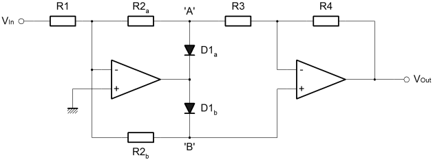 The main Op-Amp, that on the left, here has two separate feedback loops. Actually the previous circuit did too, but there the two feedback loops were different. Here they are the same, and normally the value of R2a & R2b would be the same as that of R1. The circuit is still an inverting amplifier it's just that one loop, 'A' is used when the input is positive. The 'B' loop is used for negative input voltages. Unlike before, due to the separate loops and the separate output amplifier, the full gamut of programming options are available. The overal gain can be controlled through the separate gains of the input and output circuits, and there is also some degree of freedom to control gain independent of input and output impedance. To top it off the relative gain of positive and negative inputs can be controlled separately. The basic operation of this circuit is largely the same as that of the half wave rectifier. One or other of the diodes is forward biased, the opposite diode is reverse biased. Through one or other of the diodes, the inverting input is maintained at the ground potential of the non-inverting input. If the 'A' diode conducts then the controlled "virtual ground" is transmitted to the right hand amplifier by the 'B' node. The reverse is also true. 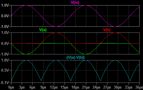 The important thing to notice, is that the potential at 'A' is always smaller than it is at 'B'. The potential at 'B' never goes below ground, and the potential at 'A' never rises above ground. In this way, the common mode value of the signal measured by the output amplifier slews up and down, but the measured value is always positive. You'll notice that in the simulation plot above I've not measured the output node, I've actually calculated the output plot from the nodes 'A' & 'B'. In the simulation the output amplifier was simply unconnected. There is a specific reason for this. The operation of the circuit is as I describe, and the plot above reflects that. The trouble is that if you tack on the output circuit, the nodes 'A' & 'B' don't behave in the way I have described. Actually what happens is that the 'A' potential does rise above zero. 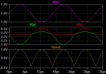 This happens because the inverting input of the newly attached output amplifier, tracks the potential on the 'B' node. This is quite proper behaviour for the output amplifier. This change in potential at 'B' then causes the potential at 'A' to rise where previously it would have been at ground. This happens by virtue of the current flowing out through R3 into node 'A'. Originally 'B' became positive because of a negative input. Now that 'A' is more positive than we expected, 'B' must be less positive to balance the inverting input of the input amplifier. Overall this is a stable manifestation of loose coupling introduced between 'A' & 'B' when the output amplifier is added. By virtue of the way the left hand circuit works, and the fact that the ouptut amplifier measures the difference between 'A' & 'B'; the output is actually correct for any given input. This is just an anomaly but it can be corrected. 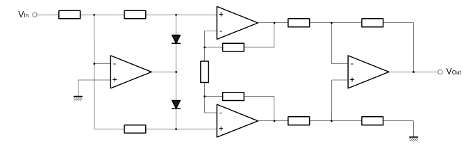 The best approach to correct would be to use an instrumentation amplifier like the AD620. Above I have shown three Op-Amps wired in the AD620, or instrumentation amplifier, configuration. Clearly with a high input impedance, the instrumentation amplifier will not couple the 'A' & 'B' nodes in any way. The previous problem is eliminated. The only real problem then, is that the cost of the circuit continues to rise as a result of the search for perfection. Since the anomaly in the simpler circuit does not have to affect the precision of the overall function, the extra cost of the more complex circuit seems unjustified. |


Copyright © Solid Fluid 2007-2025 |
Last modified: SolFlu Mon, 08 Apr 2013 22:27:36 GMT |