 |
 |
 |
 |
 |
 |
|
Differential Line driver
Obviously we're going to be using OpAmps to drive the line. All of these articles are all about Op-Amps. Since the line driver is made of amplifiers, the line driver too is a kind of amplifier. The diagram below demonstrates just such an amplifier. For the purposes of what I describe here, we'll be considering the driver amplifier as individual Op-Amps and passive components. An amplifier like that below can be purchased as a single device typically SSM2142 or DRV134. As we'll see, many of the resistors in this amplifier intentionally have similar values. These similarities are essential to the balanced behaviour of the amplifier. I've written about how we are converting a single ended voltage input into a voltage difference between the outputs. Although the overall gain of the amplifier is important, much more important here is that the outputs precisely signal equal and opposite potentials. The gain balance is a critical parameter. If the two signal lines exhibit phase or gain differences, these will degrade the integrity of the differential signalling scheme. Although the commercial monolithic product is more expensive than the Op-Amps and resistors that could replace it, usually it's not worthwhile. The valid and good reason that these commercial products are abnormally expensive, is that the internal resistors are individually laser trimmed. Each and every chip is calibrated before it leaves the factory. This is worthwhile and beneficial because it ensures good gain balance and low distortion. 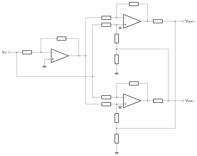 The amplifier is a good deal simpler than it may look. Actually it's three amplifiers, two are the same, and all are of types that we've already covered. On the left is a single inverting amplifier, with equal value resistors to ensure unity gain. The basic function of this amplifier is to provide equal and opposite versions of the single ended input signal. This amplifier actually calculates the difference which is signalled at the output. Although we have equal and opposite signals from this first stage amplifer, their source impedances are very different. The positive half of the signal is literally the amplifier input signal with unknown source impedance. The generated inverse has the output impedance of the amplifier output circuit. These different source impedances will certainly affect the gain balance and are obviously not acceptable signals for direct connection to the line. We need to buffer these signals.On the right are two identical amplifiers, one for each of the positive and negative outputs. If you look carefully you'll see that the inverting input to one of these amplifiers is connected to the non-inverting input of the other. In this way the polarity of the outputs is defined as opposite. Quite importantly, the outputs of these amplifiers on the right hand side are cross coupled. Although important, for the time being just ignore the cross coupling and assume that nodes 'A' and 'B' don't exist. Imagine that the resistors either side blend into one resistor with value equivalent to the sum of the originals. That way, these two rightmost amplifiers are simply differential amplifiers with an output damping, or source matching impedance. In this imagined configuration without the cross coupling the gain of each differential amplifier is just over two. If the resistor around the eliminated node had the same vaule as all the others in the circuit, then the gain of the differential amplifier would have been exactly two. What is important, is that when the circuit is connected as shown in the diagram with the cross coupling, then the gain of the differential amplifer is reigned back to exactly one. The reason for explaining this in such a convoluted way, is to demonstrate what the cross coupling is doing to the amplifier. Remembering the differential amplifier, this new action is reasonably intuitive. Below, the diagram isolates this new amplifier which I would describe as a "modified differential amplifer". To simplify things, I've replaced the cross coupling with an "invert function" wired from the output of the same amplifer. Both the positive and negative amplifiers were identical so their outputs should inherently be equal and opposite magnitude for any given input. I hope it can be seen that this is functionally equivalent to the inverter wired from the output, but significantly easier to deal with when it comes to the derivation of equations. The damping resistor (RDAMP) can more or less be ignored. It's main function is to match the amplifier to the transmission line. It overcomes the tendancy of the amplifier to drive excess current into the line (or sink it from) when a transient or edge is placed on the line. This happens because the line can have an apparently low impedance when actually its real impedance is the characteristic impedance of the line. The extra (or the deficit) electrons on the line will inevitably show up at some other point when you don't want them to. This only happens on long lines when it takes some time for the actual signal to propagate the length of the line and thus for the line to show its true impedance. Typically the value of the damping resistor would be small and can can be ignored here, because we're interested in the behaviour of the amplifier and not the line. The load resistor (RL) too can be ignored. Obviously the load resistor is primarily driven from the amplifier output. The output of the amplifier is a controlled voltage. All the load resistor does is to limit the current when the output is referenced to a foreign, and possibly elevated, ground potential. In theory there is actually no need for this resistor, since the amplifier will control its output voltage in an explicit way. The output will source or sink extra current for the benefit of the non-inverting input. The load resistor helps with stability, EMC and reliability. 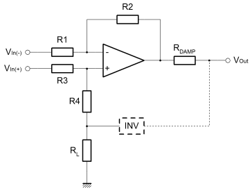 The inverting input of the differential amplifier, does as it always did. R2 ensures equivalence between the inverting and non-inverting input voltages. In turn, this action controls the output voltage in proportion to Vin(-) through the current developed in R1 and R2. Vin(+) also has influence over the output because it sets the voltage on the inverting input, and therefore indirectly the current in R1 and R2. This is all the normal thinking developed in the page on linear operators. Then, because Vin(+) and Vin(-) are equal and opposite it's reasonable to assume that the gain is two. The non-inverted signal will make it through intact, and the inverted signal is subtracted. We are adding two identical signals, or perhaps subtracting a negative version from a positive one. Either way it's the same. In the differential configuration the non-inverting input to the amplifier shows a voltage which is half that of the input signal. Of opposite polarity, the inverting input signal must cause a current in R1 which is double that which it would be, were the non-inverting input grounded. If the current in R1 is double then so must the output voltage, by virtue of R2. When the cross coupled ouput is connected, it's like adding another inverting feedback path. Actually this feedback path should cause the non-inverting input to the amplifer to be at ground potential. To do this, the amplifier output must be equal and opposite to Vin(+). If you look, it can be seen that this is the only possible stable condition. The inverting input gain term overrides the attenuation due to the cross coupled feedback path. The combined gain is thus limited to one when the output is too big for a given input. The other way; if the output becomes too small, then both the inverting and non-inverting inputs can contribute their gain terms to the output. 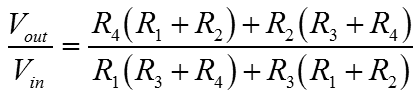 If the non-inverting input is zero, then the gain must be one, but it only applies if all the resistors (except RL and RDAMP) are of the same value. I did wonder about this so I derived the function just to be sure. I'm not going to put the working here, but you can find it as a PDF in the working section. |


Copyright © Solid Fluid 2007-2025 |
Last modified: SolFlu Fri, 29 Mar 2013 02:10:25 GMT |