|
Design Specification
Before we dig into the details it's quite important to simply set out a list of basic requirements that the UART will need to satisfy. Most of these things we have mentioned along the way. I've just re-listed them for the purpose of completeness.
- Coded in VHDL.
- Built from common components.
- Interface on the RS232 side with existing technology.
- Where necessary, communicate with identical module.
- Support variable Baud rates including 1200, 2400, 4800, 9600 and 19200.
- Provide only for 8 data bits, no parity and one stop bit.
- Provide "Auto Baud" detection.
- Provide an inner interface which is easily compatible with both programmable logic, and microprocessor bus interface.
- Provide a busy signal on the internal side of the transmitter.
- Provide Baud and Data available signals on the internal side of the receiver.
- Provide Metastability avoidance on the external interface of the receiver.
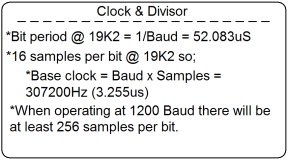
- Operate from a 307200Hz clock.
The final point which isn't listed above but is pretty much implicit from the perspective of creating a functional design, is that the transmitter and receiver clocks should essentially be asynchronous. Within the bound of the test harness we'll describe later, it will be unnecessary to actually test this because the design approach we'll take will ensure that this asynchronous requirement is met. The diagram below shows this requirement quite clearly, and provides a clue as to how we will actually achieve it.
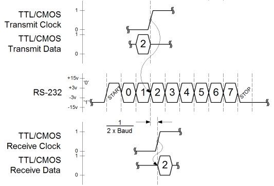
The upper part of this diagram shows bit two of the serial data ready for transmission. Then, the curly arrow shows it being transferred from inside, to outside, the transmitter on the rising edge of the transmit clock. It is implicit that all of the data bits are transferred on to the serial line in this way. Perhaps more importantly the lower part of the diagram shows the receive clock offset from the transmit clock. Ideally this offset is half of a single bit time. When the receive clock goes high then the receiver has captured the bit.
The basic strategy for sampling data on the receiver is that the receive clock runs at least sixteen times faster than a bit period. Because of this there are sixteen opportunities during each bit, when it is possible to capture a bit. We can never capture the data bit exactly centrally, but we can within at least a sixteenth of a bit period.
So let's cut to the chase. I'm not going to work through the whole design, character by character. It seems to me that some rationale and philosophy is useful, but when it comes to the nth degree, you either get it or you don't. I'm not going to leave it all to faith, however.
The design breaks down into three basic modules; The transmitter, the receiver, and the test harness. More or less, these are all derived from architectural components which I've hived off into a component library. This was a conscious decision from the perspective of this article as an example. I've explained that VHDL is quite like a normal programming language in some ways, but not in others. I feel that if you're new to VHDL, you'll see the programming language aspect of VHDL, and how it can be expanded to speed development.
Most significantly, if I had simply implemented the whole UART in one file, with no architecture, the peculiarities of the VHDL entity/architecture relationship would not have been so clear. Possibly more significant is that most graphical VHDL entry tools will produce these constructs automatically so it is important to understand them for when one inevitably has to unravel computer generated VHDL!
I'll look at, and contrast, the transmitter and receiver. Then I'll explain the design of the most common component of the design, the Multifunction General Register. I'll talk about the design of the two state machines that drive the logic, and finally I'll do a brief on the use of test harnesses.
|