|
Test Harness
The test harness is a pretty important part of any module, particularly in VHDL. There are two basic methods of testing. In either case the newly devised module is essentially started and taken through a comprehensive sequence of operations. The simpler solution for evaluation is a "white box" visual inspection of the unit under test, in the simulator. VHDL also has an extensive library capability for dealing with disk file input/output, much like one would expect of any normal programming language. Obviously for the purposes of actually synthesising logic gates in a semiconductor device such capability is not useful, but when it comes to implementing test harnesses for complex VHDL modules it is nearly indispensable.
In broad terms the file I/O approach to testing is often not particularly useful for initial testing. In the circumstance where a developer has a hierarchy of design units, perhaps each might contain a state machine and some resources. If the developer has an overall specification, it would be natural not to have detailed internal specifications. If the coding of the component design units is not complete, there is not much point in developing a complicated file I/O test harness.
In equal terms, when a design reaches the SoC (system on chip) level, there are two problems which render the casual stimulate/inspect test regime ineffective. The first of these problems is that it is probable that more than just a small few people are involved in the design of the project. In this kind of case, it's just not possible for any one person to come along, look at a few waveforms and be able to say that the system is functional with the right degree of certainty. The second problem is that once a design has reached the size of a moderate SoC, it's actually a very complex system.
Unless there is some sort of hardware verification scheme in place, simulating an entire SoC, on a computer can take many hours of compute time. Where hardware verification is in place, it cannot always be used simply because it makes access to the internals of the design so much more difficult than the simple software simulator. These constraints make file I/O testing regimes more important. Typically test vectors, and results can be listed for automatic go/no-go comparison. Equally it is also possible to use text messages which assist with complex debugging.
 |
Writing to the transmitter |
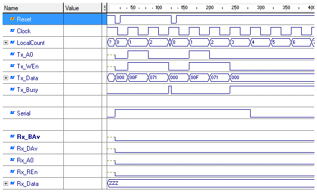
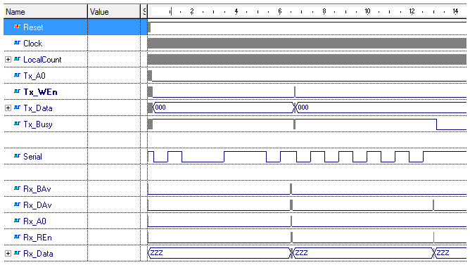
Our little serial port is not grand enough to require a complete file I/O test harness. In this case I have adopted the approach where a sequence of test vectors stimulates each of the basic functions that the unit offers, but does not attempt to exhaustively test the functionality of the unit. The verification method is through simple inspection. I have witnessed that the behaviour in the timing diagram, is followed.
To make the tests easier to describe, I have used the transmitter and receiver connected directly to one another. This is possibly not the best idea for a final test since it does not categorically verify that both the transmitter and receiver will work with a standard UART. This example code was programmed from scratch, however, I have used an identical concept previously and that seemed to work without hesitation, so I feel confident that this design ought to be O.K. That said, it's not really a good enough approach for silicon target, but for a programmable logic target, it's fine.
The beauty of test harnesses is that you need to be far less careful about your coding style. When programming state machines or combinatorial logic, it is simply not acceptable to describe functionality which relies on wait statements and their kin. When simulating the implementation of a design in a semiconductor technology, the synthesis and/or place and route tool may back annotate the design with technology representative delays, but this is different altogether. Out in the realm of the test harness, one can let ones really dodgy programming desires run riot! In some cases, like the generation of clock and reset, it is impossible to generate these signals in the simulator without explicit delays.
The test harness then is actually pretty simple. The reset and clock signals are generated in separate loops. The reset loop is designed to generate a pair of pulses, which helps to verify reset functionality when the design is running and not just uninitialised. The reset loop is designed to get "stuck" after these pulses have been generated. The clock signal is generated in a different loop, and it runs infinitely from before reset. The actual cycle time for the clock is in the order of picoseconds. This sort of cycle time is far faster than we would ever expect, or desire, for the serial port. It is arranged around the delta delay for the Aldec simulator I used. This simulator seems to have a fixed delta delay due to it being evaluation/student software.
 |
Full serial data stream |
The delta delay is the simulation infinitesimal. This is the step time interval on which the simulator evaluates all of the signals in the design. Clearly this could be event driven, but in the case of the evaluation version it appears not to be. With such a small infinitesimal, and with such a comparatively slow operating function like the serial port, it is highly desirable to bring the base clock somewhat closer to the infinitesimal. This helps to speed up the simulation. The accuracy of the simulation is not affected because it is, internally at least, a fully synchronous design. If we were to target the serial port at an FPGA, and then back annotate the technology delays into our design, it would then become important to have the clock set accurately to it's intended frequency. This is clearly difficult with the student/evaluation version of this software.
On this basis I assume that Aldec will not require me to pay for their software, since I have not targeted this design to an FPGA. I would also recommend this software to you. It seems to me to be at least as good as the Modelsim/Renoir combination from Mentor Graphics I used some 10 years ago. In particular, and even then, the software had more functionality than I needed. In fairness to Mentor, software does generally improve with time. Most significantly it is not clear to me that Aldec have tool chains to route a design to either FPGA, or Silicon, as mentor do with Leonardo Spectrum and Olympus SoC. Irrespective I would imagine that the Aldec design and verification tool is a superb alternative, to the Mentor offering if one is not already tied into the Mentor Design Architect tool chain.
The remainder of the test harness is nearly as simple as it gets. A counter is provided as a reference for the test vectors. The test vectors themselves are issued from generators which look at this reference counter. The vectors were coded by inspecting the response waveform in the waveform viewer. Once an operation or event occurs and is verified, it is possible to select and describe a new vector, to slot into the vector generator. Once all of the necessary vectors have been supplied and the waveform is as expected, one can be satisfied that the functionality is good. When the result is good, it is appropriate to capture the results for use in later automated tests. This might be done by VHDL file I/O, and would allow the unit to be checked, even after subsequent modification.
That just about concludes this series on my UART. I hope it has been interesting and perhaps educational.
If you have got this far, thank you for persevering, and happy hacking! |