 |
 |
 |
 |
 |
 |
|
UART Synthesis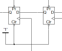
The approach to synthesising logic for this transmitter and receiver is much the same as for any fairly well defined function. In broad terms one must work out what resources one will require, in respect of the data path. Typically most complex functions will have some element of timing. The overall control signals will be abstracted from the core function to the extent that some form of complex control will be required. The data path would normally take the form of a group of registers, multiplexers and other combinatorial functions. Some of these resources will inevitably be sequential, like counters. Often arithmetic functions like multipliers will be pipelined, for efficiency and speed. Usually a central state machine will co-ordinate these resources in the data path, to produce a useful result. This is achieved by managing pipeline and other sequential delays to make the overall control functions intuitive, and easy to use. Now is probably a good time to check out the schematics for both the transmitter and receiver. If you're following the text perhaps it would be beneficial to print them out so you can look at the diagrams and read this text at the same time. I've just described that it's normal to have some sort of state machine in the middle of a general function, and these can be seen clearly on both the transmitter and receiver schematics. In these general terms the transmitter and receiver are remarkably similar. The main common components are the counters and registers along the bottom of both diagrams. These are associated with maintaining an understanding of the point in time relative to a processed byte. 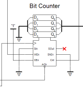
Both transmit and receive have a sample counter. This sample counter is arranged to be zero at the beginning of a bit period, and it counts up during a bit. The Baud rate register provides a reference for the sample counter, and when the sample count matches the Baud rate divisor the bit is complete. A comparator is used to generate a flag which indicates the end of the bit to the state machine. The state machine manages resetting of the counter and ensures that the count goes from terminal to zero at the exact edge of the bit period. Also common is the Bit counter, which like the sample counter is controlled by the state machine. The bit counter is responsible counting the actual bit periods and determining the overall time point of the incoming word. The bit counter is referenced against a constant value to generate a stop flag for the state machine. Also common is the shift register shown at the top of the page. The shift register is responsible for converting a parallel data byte into serial for the transmitter, and vice versa. The direction of parallel to serial conversion is different for the transmitter and receiver, hence slightly different wiring, but the basic function is similar. In both cases the state machine is responsible for controlling when the shift register shifts. In the receiver the state machine indicates when data is ready, and in the transmitter, the state machine protects the outgoing data against inadvertent modification during transmission. In the transmitter data and baud rate can only be written. This is done by making a selection with address bit zero and then applying a write enable pulse. On the receive side Data and Baud rate can only be read. This is done in a similar manner to the writes of the transmitter. When the transmit and receive are combined for the full UART capability it is the responsibility of the user to detect, read and transfer the baud rate from the receiver to the transmitter. Overall the transmitter is slightly simpler than the receiver. The most significant function, unique to the transmitter is the output control mux. This gives the state machine control over the output, to specific logic levels during idle, start and stop bits. Since the last thing before the serial output is a multiplexer, a final flip flop is used to keep the output signal edges clean. It is common that a multiplexer will select various inputs during a change from one output to another. This can lead to unwanted edges, which the cleanup flip flop eliminates. 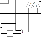
The receiver has a tri-state buffer on it's data output. This is not always necessary, but it's inclusion allows the receiver to become one of many devices on a shared bidirectional bus. The receiver has an optional divide by two on the Baud rate divisor, although on the user read bus only the full Baud rate is seen. The divide by two allows an offset into a received bit to be made. Typically we will trigger reception at the beginning of the start bit. Although individual samples will be at bit period intervals, we must offset by half a bit period in order to sample the bit in the centre of the bit period. The receiver has a key detector on the shift register output. This comparator references a fixed constant, and indicates to the state machine that the Auto Baud Key has been received. The state machine knows if it previously had a Baud rate divisor, and can act to confirm the new Baud rate in the circumstance that it did not. Finally the receiver has two metastability avoidance registers. The use of flip flops in this way is a common technique to avoid sampling problems on inputs from the outside world. When a clock edge is received at any flip flop and the 'D' value is indeterminate it is possible for the output of the flip flop to oscillate. This is undesirable, especially if the output of the flip flop feeds combinatorial logic. Potentially the combinatorial logic will oscillate in turn, and lead to a greater possibility of other flip flops becoming metastable. A typical flip flop that experiences such conditions will not oscillate forever. By simplifying the input sampling to just these two flip flops, the maximum settling time for the flip flops is afforded. Considerations of pipeline delay are especially easy to deal with in this design since the external interface is just a single wire. In more complex designs one has to consider the pipeline delay of metastable compensation quite carefully, in order to maintain balance. I'll say more about this later. That pretty much wraps up the design for the transmitter and receiver. The internals of the controller machines are slightly more complicated, but we cover these separately later. Next we'll look at the general register. In this design the general register is the backbone. It has five simple functions, and is used variously for counting shifting and storing. |


Copyright © Solid Fluid 2007-2025 |
Last modified: SolFlu Sat, 24 Oct 2009 04:45:18 GMT |