 |
 |
 |
 |
 |
 |
|
Making the PCB (Part 4)Having completed the etch process, and cleaned up the mess, we can move swiftly on to completing the board. We have a piece of fibreglass, and it has the tracks we want on it. Unfortunately, it has the toner and the carbon film polymers that we used to define the tracks on it. We have to remove that, and it will come off easily with Acetone. Goop RemovalYou can use the IPA cleaning rag, or a new rag, it doesn't matter. The only notable point with this stage is to try and wipe the "goop" away from the middle of the board. Don't work around in circles. Also try to keep a clean(ish) patch of rag doing the actual cleaning. The problem is that the fibreglass is moderately absorbent. If you leave the toner and "green" on there to dry, it's difficult to shift. It won't affect the board at all, but if you hold the board up to the light, you'll see the streaks left on the board. 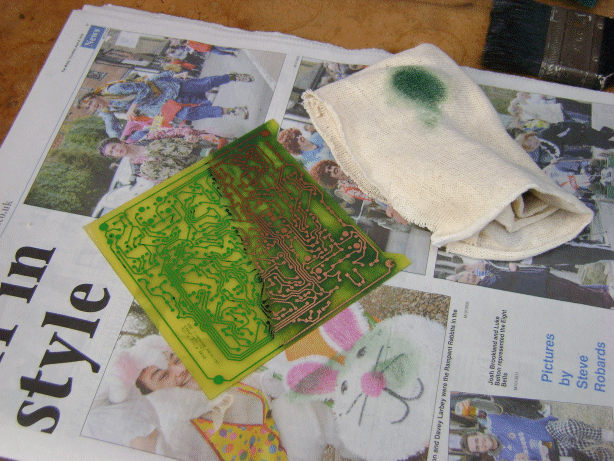
The picture above shows the process, and in this particular image I've done half the board, for effect. In this case I'm wiping from the middle to the sides. You can see in the image that I've gone too long on one patch of the rag, and green is soaking into the board. Also you can see the copper shining through once the toner has been removed. In practice, it's a good idea not to remove the toner, until you're ready to tin plate the copper. The toner helps to prevent the air from getting at the copper. Once it's tarnished, it's more work to clean up for tin plating. Once all the toner has gone, it's probably worth looking at the tracks to see how tarnished they are. In any case it's not hard to use ScotchBrite to polish them up. If you do polish, then a drop of IPA again will lift any muck off the surface. Tin PlatingThe tin plating is done with Stannous Chloride, or Tin(II) Chloride. They're the same thing, but two different names. This stuff again is not hugely harmful, but goggles and gloves are a must. As with the Ferric Chloride, it's worth having a bucket of fresh water around to rinse your gloves. Tin Chloride doesn't seem to stain, but it smells awful. Generally it's more difficult to get hold of than the Ferric Chloride, but you can certainly get it online in the UK. Because it comes in the post, it comes as a powder that one mixes with water. Obviously as a powder, it's more easily manageable; clearly the powder is potentially more dangerous when in contact with skin. The moisture in the skin causes the concentration to be higher than if one were to correctly dilute it. The normal method of distribution is that a small quantity of the powder arrives in a large plastic bottle. The idea is that the bottle is of such a size as to contain the correct amount of water for and accurate solution. When mixing the water with the powdered crystals, the water must be warm, or the crystals won't completely dissolve. As soon as the solution is made, it will start to go off. It has a lifespan of around six months. The solution will plate better if it's warm, so a warm day yields better results. I have another plastic pan, like the one I used for the etch process, dedicated to the tinning process. When the tinning is done the solution can be put back in the bottle and used again. At the end of its life, you'll probably have around a litre of the Tin (II) Chloride to dispose of. For that quantity, it's worth disposing of it properly. Take it to the refuse tip and ask what to do with it. 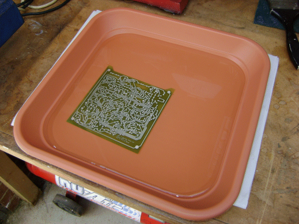
The picture above shows the board in the tinning solution. Usually I might leave it there for a couple of hours, but it's normally good to go in about ten to fifteen minutes. If you're going to leave it for any time, it's worth covering the solution, so that the smell doesn't spread!! DrillingOnce you're happy with the tin plating, rinse the board in fresh water and inspect it. Assuming everything looks good, you're pretty much ready to drill the holes in the board. 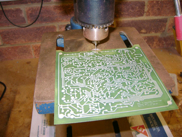
The picture above shows the board on my drill press. The majority of the holes are the standard 0.032" (0.85mm) diameter ones. This is pretty small, so the drill will have to be set to a fairly high speed. I got ten of these drills, in carbide, for about £8 on e-Bay, which is pretty good. The carbide is good because the glass fibre is very abrasive. Normal HSS drills won't take the grief for long, and unless you have a cutter grinder, small drills like this are almost impossible to sharpen at home. The high speed is important because the drills are very brittle and break easily. You'll need at least 1000rpm. My drill press is a bit big for this job really, but it goes up to 2000rpm, and that seems fine. 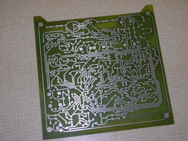
I'm sure everyone is going to have a different take on this, but through trial and error I came up with a fairly good method for getting the holes on target. Obviousy in a production environment this stage would be done by a robot, but we don't need all that. Using the pads as a guide, it's quite possible to get the holes in the right place. At least, well enough that it's not a problem. It's unusual for me to say don't bother marking out. In this case it's just impractical to do marking out. If you get the light right, the drill point will cast a shadow on the board. You just need a good lighting tube, above and to the side of the press. Set the point of the drill around a quarter of an inch above the board. Any lower, and you'll break the drill too easily when you insert and remove the board. From there, don't bother with the lever on the press. Try to operate the quill of the drill as close to the centre of rotation as possible. It should be possible to flick the drill through the board with a tiny movement of your fingers. Arrange for the drill to hover above the board by about a millimetre while you position the board each time. By hovering, and flicking you'll get around the board pretty quickly. Most significantly, the closer the drill point is to the board, the more accurately the shadow casts on the pad. From there you can see that the shadow is in the middle of the pad. It doesn't take much practice to get pretty reasonable results. If you get it a bit wrong, don't dwell just keep going. If you get it badly wrong, keep going until you get it right. The worst possible case is that the drill severs the connection between a trace and a pad. Visual inspection will highlight these problems, and they can be corrected with a careful dob of solder, when the components go in. One area to take care of, is the holes for pin header arrays. Even if you're doing an SMT board, you'll likely have these. The pins are slightly larger than those of a standard through-hole component. You could obviously get another drill size specifically for them, but it's not necessary, because the standard 0.032" (0.85mm) drill will suffice. The only problem with the smaller holes is that you must get them in a dead straight line. The larger pins, in a straight line, won't be happy about going through holes that aren't quite right. If you're new to this, do those holes last or setup some practice examples first. The same idea doesn't seem to apply to IC sockets. The pins are smaller. The bigger holes and pads are more difficult to judge. I found that with these the best plan is to lightly drill into the surface of the board, where it looks right, and then drag the board out for a closer look. Because the mark is already there, the second time it's easier to judge where the hole should actually be. Obviously it doesn't matter if the surface is marked. The 0.032" (0.85mm) drill is so small that any other drill will destroy the erroneous marks, and follow the main hole. As the hole size gets bigger, it's easier to judge how far off centre you are. If you go up in stages gradually, it's possible to get the hole pretty nearly dead centre, because the eccentricity shows up so clearly. 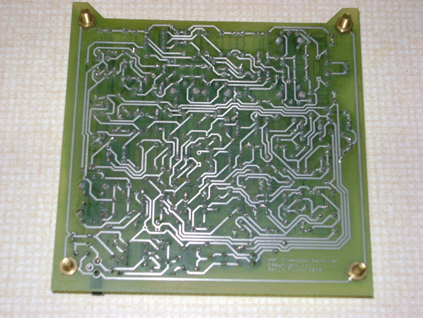
AssemblyThe pictures above and below show the (more or less) completed board. Assembly is reasonably straightforward. If you want to, you can produce a "silkscreen", with the reference designators for the components. It's seriously helpful when you come to stuffing the board. You can put this on the component side of the board, much like the etch resist for the traces. Be sure to clean the fibreglass in the same way as the copper. If you don't the toner won't stick. The typists carbon film, is available in many colours, including white. The white one is ideal for making the silkscreen stand out, but it's not essential. With single sided boards I like to modify the component side copper Gerber file by removing the pads in my text editor "Osmium". This just leaves me with the traces which represent the wire links. These can then be merged with the silkscreen Gerber data, to produce a composite image that includes the reference designators, component outlines and the positions for the wire links. With so many holes, it's difficult to keep track of which hole you need when stuffing the board! If you're going to do a silkscreen, then obviously do it before the components go in. The board won't go through the laminator once it has components on it! When soldering the board, stuff (or solder for SMT) the low profile components first. It makes it easier to hold the components in the board when you turn it over. Obviously the tallest components will be resting on the bench when you do so. If you put tall components in first, you'll have a devil of a job to get shorter components to lie flush on the component side of the board. When the soldering is complete, just use a drop of the Isopropyl Alcohol with an old toothbrush to remove the flux residues. If you don't they'll rot the board over time. Try not to get too much of the IPA on the component side of the board. It's not terrible, but it will tend to degrade the "silkscreen" if you used one. 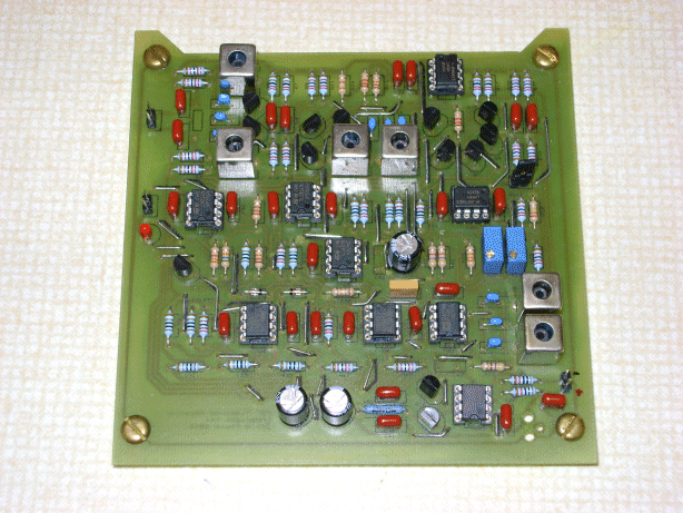
In conclusionThat's it. It's easy, and pretty cheap. Give it a bash! I don't think I'll be bothering with stripboard any more, except for the smallest of circuits. From an electronics perspective, PCB's really are technically better than stripboard. I think they're easier to modify, and they look far more professional. You also get the opportunity to place components and choose the constraints on your circuit. With stripboard, it's almost "luck of the draw". Double sided boards are more complex, but they can be done. Perhaps if one was feeling really enthusiastic, a four layer board would be possible. The only real problem remaining is that of vias. I have avoided those problems on this board by simply opting for a single sided design, with wire links. I think that makes most sense anyhow for a small prototype. I have seen people working on solutions to the via problem that close the gap between wire pins, and proper through hole plating. Such solutions can work, and they typically use silver loaded conductive paint. For me that seems a bit messy, and it really isn't cheap. For me that's not a realistic route. Having come this far, I think I might be thinking hard about alternatives, however. I hope you found these pages inspiring and informative. |


Copyright © Solid Fluid 2007-2025 |
Last modified: SolFlu Sat, 03 Jul 2010 12:14:25 GMT |