 |
 |
 |
 |
 |
 |
|
Low Cost Prototype PCBs
If you're anything like me, you'll have built quite a lot of stuff on Veroboard or stripboard. There is a class of circuit designs that don't really warrant having a professionally manufactured circuit board, but equally really do need to be made. This class of circuits, includes test harnesses for production units, experiments and interesting side projects. For some, perhaps breadboard is the answer. I've never been a fan of breadboard. My main concern has always been that with a lifetime of abuse, normally stored in a box in the loft, elevated temperature, cold and damp, the connection strips in breadboard oxidise in a vicious way. The problem with breadboard, is that it's not that easy to get the component gripping conductive strips out, in order to clean them up. It always seems to end up being a triumph over adversity making electronic circuits work properly on breadboard. If it's not the breadboard it's self, then it's the thousands of odd used components that collect in little plastic bags. Those are the ones that have been used just a few too many times. Stripboard is significantly superior to breadboard. It allows one to build a circuit to almost infinite complexity, and with proper soldered joints. They always conduct. Sure, you can't reuse the components as easily. If you're reasonably sure that your design is good before you put it onto stripboard, then it will certainly stand the odd resistor change, perhaps even a "rip and reroute" to use the same circuit with a different IC. For a long time stripboard was my first choice for this class of circuits. The choice was probably less to do with benefits of stripboard, and more the unsuitability of breadboard. Fundamentally, when you do get your circuit working, breadboard is a dead loss. If you actually want to use the circuit, breadboard, being a complex plastic and metal assembly, you can't chop it up and put it in a box. Even if you did, one could never be sure that the components hadn't fallen out.
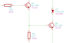
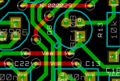
Focussing then, on the disadvantages of stripboard, it's not hard to find a few. Probably the most basic, is the linear nature of stripboard. Although in theory it's quite possible to built infinitely complex designs on stripboard, they always end up being huge, and peppered with wire links. Because of the linear nature of the copper strips, one seeks a consistent strategy for routing the circuit, and it always end up being a scheme where each IC occupies a regular space. The surrounding space is then gradually populated with the smaller passive components. Finally the wiring, is squeezed in around it all. With more complex designs one tends into using wire wrap. Wire wrap, is, or rather was the ideal solution, especially in commerce and the military, for low volume complex circuits. One can place components almost as one wishes, and the wiring on the back is fine enough to take care of everything else. The big problem with wire wrap is that it is actually quite expensive, since the pins on the reverse must be long and specially machined to grip the wiring. It's still just as time consuming and intense to actually wire up, as all the preceding schemes. For design changes, wire wrap is possibly the worst approach of all. It's inevitable that the wires of interest are at the bottom of the "nest" For me, for a long time, the answer was to use a solder based version of wire wrap. Using enamelled wire, if one was careful, one could use ordinary component sockets in conjunction with a "pad only" matrix board. The enamelled wire gives way to the heat of the solder. All one has to do is wrap the wire around a pin, and finally touch it with solder for a good permanent join. It avoids the cost of the special wire wrap sockets which are expensive. In truth, none of these schemes are particularly attractive for a low cost solution. One would always end up looking wistfully at the low volume prices of commercial PCBs, contemplating the possibility of home made PCBs. The main problem here, is that the whole process is quite lengthy, and involves multiple stages of etch resist, and etching. You need a UV lamp, and then all the problems of getting the etch resist to stick. Chemical aging. Etching tanks. Hassle. Now, the whole thing has been completely smoothed out. There is a PCB route. It's quick, effective and cheap. It produces accurate copper tracks right down to 0.008" track and gap rules. You can leverage the really comprehensive free PCB design tools, and you get a board that is as easy to make at home in small quantities, as it is to have made commercially in large quantities. This series of pages, is about just that scheme. Open your eyes and never go back. All that old stuff, it's just not needed any more. The cheap hand made prototype PCB answer has arrived. |


Copyright © Solid Fluid 2007-2025 |
Last modified: SolFlu Wed, 07 Jul 2010 10:11:20 GMT |